Edit Symbol Fields: The Ultimate BOM and Component Data Manager
Exploring the “Edit Symbol Fields” View in KiCad’s EEschema
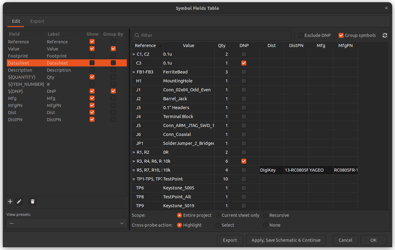
KiCad’s EEschema tool is a powerful, open-source schematic capture program that is a part of the KiCad suite. One of the standout features within EEschema is the “Edit Symbol Fields” view, which provides a comprehensive interface for managing the properties of symbols used in your schematic designs. This makes editing component data like BOM information or population options simple - you can easily add BOM info for multiple components in parallel! Here’s an overview of what this view offers and how to make the most of it.
What is the “Edit Symbol Fields” View?
The “Edit Symbol Fields” view in EEschema allows users to view, edit, and manage the fields associated with each symbol in their schematic. These fields contain essential information about the components, such as part numbers, values, footprints, and other custom attributes.
Key Features and Benefits
At first glance, this isn’t much more than a glorified Excel spreadsheet. However, this is an extremely powerful and time saving view.
- Centralized Field Management:
- The “Edit Symbol Fields” view consolidates all fields for all symbols in one place, making it easy to manage and edit information without navigating through individual component properties.
- Bulk Editing:
- This feature enables bulk editing of fields across multiple symbols. This is especially useful when you need to update the same field for many components, such as changing all resistor values or updating manufacturer part numbers. Gone are the days of hunting down every single 10k resistor in the design to update the manufacturer part number!
- Custom Fields:
- Users can add custom fields to symbols, providing flexibility to include additional information like supplier details, prices, or custom notes. These custom fields can be used for better documentation and BOM (Bill of Materials) management. A great example of this is population information. Before Kicad added the “Do Not Populate” attribute, adding a “Pop” field in the attributes table was a common way to manage DNP components.
- Filtering, Sorting, and Grouping:
- The view allows for filtering and sorting symbols based on different criteria. This makes it easy to locate specific components and manage large schematics efficiently. It also allows for effective grouping of components by fields like population, dielectric, power rating, voltage rating, and much more!
- Footprint Assignment:
- You can assign or change footprints for multiple symbols directly from this view, ensuring that each component is correctly represented in the PCB layout.
- Export and Import:
- Fields can be exported to and imported from CSV files. This functionality is useful for BOM generation and for integrating with other tools or databases. Note that exporting is significantly simpler than importing; while an export can be handled through KiCad, an import must be done by copy/pasting fields from an external spreadsheet into the fields view.

Want to support KicadTips?
Consider purchasing EE tools or supplies through our Amazon affiliate links. You get quality items at no extra cost, and we earn a small commission.
Whether you need an oscilloscope, solder, or jumper wires - every purchase helps!
How to Use the “Edit Symbol Fields” View
- Accessing the View:
- Open your schematic in EEschema. Navigate to the top menu and select
Tools > Edit Symbol Fieldsto open the view.
- Open your schematic in EEschema. Navigate to the top menu and select
- Viewing and Editing Fields:
- The view displays a table with symbols and their associated fields. You can directly edit the values by clicking on the cells. Use the toolbar options to add, delete, or modify fields as needed.
- Bulk Editing:
- Select multiple cells or rows and use the right-click context menu to apply changes to all selected items. This is ideal for making uniform updates across several components.
- Adding Custom Fields:
- Click on the “Add Field” button to introduce new custom fields. Specify the field name and value, and apply them to selected symbols.
- Filtering and Sorting:
- Use the filter and sort options at the top of the columns to organize and locate symbols based on specific criteria, such as value, footprint, or custom field entries.
- Exporting and Importing Fields:
- Use the
Exportbutton to save the fields to a CSV file. You can edit this file externally and re-import it. Note: re-importing is a manual process. Take care to match that your modified data is easily mappable to the fields in your table!
- Use the
Conclusion
The “Edit Symbol Fields” view in KiCad’s EEschema is a versatile tool that enhances the efficiency and accuracy of managing symbol properties in your schematic designs. By offering centralized management, bulk editing, custom field support, and easy export options, it simplifies the process of maintaining consistent and detailed component information. Leveraging this view can significantly streamline your workflow and improve the overall quality of your electronic projects.