PCB Features for Faster Test and Debug
PCB Features for Faster for Test and Debug
When designing circuit boards, incorporating features that facilitate bringup, testing, debugging, and bodging can significantly streamline the development process. Here are some of the most valuable additions you can make to your board designs:
0.1” Headers
Using 0.1” headers can simplify connections with scope probes and logic analyzers. Instead of struggling to attach a probe to a pin, you can easily slot a header with a 1k resistor onto a digital bus.

This method is particularly effective when using Saleae logic analyzers. However, it is pretty space intensive. A reasonable compromise is often to include features like this in early circuit board designs, which aren’t form factor constrained.
Test Hooks as Test Points
Test hooks are a godsend when you have to attach multiple probes onto a circuit board. Tasks like testing power sequences, reset timings, or clock startups become much easier when one of the signals involved has a test hook. Using a probe witch hat, you can simply clip a probe on to a reset signal or power bus, and have a stable timing reference for the rest of your measurements.
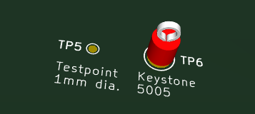
Keystone 5005 test loops provide convenient points to hook probe witch hats onto. These loops make it easy to connect test equipment to your board without hassle, ensuring accurate measurements and reliable connections. Note that it’s sometimes helpful to differentiate these symbols in your schematics as well:
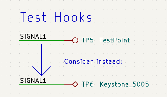
This way, you can keep track of which test hooks are physical connections rather than PCB features.
For low-speed signals, Keystone 5019 test loops are excellent for ground hooks. They offer a stable grounding point, which is essential for accurate signal integrity and noise reduction. They are also surprisingly durable due to their large pad contact with an underlying plane.
Coding Your Test Points
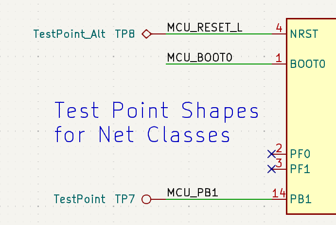
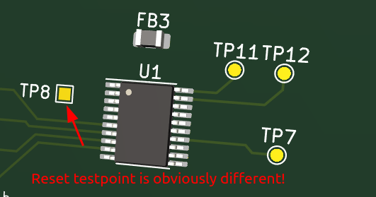
Since we’re on the subject of test hooks: another convenient trick for test points is to use different varieties of test points for different applications in your circuit board. An easy, no-cost way to do this is to assign shapes to test points based on their purpose. For example:
- Square Test Points: Use for Reset or Enable lines.
- Round Test Points: Use for general signals and traces. This makes it easy to quickly identify specific signls of interest on your boards. It gets even simpler when you add the physical context of the part with the testpoint: placing a square test point close to a chip is a clear way to direct the user to the reset signal for probing.
This approach works just as well for physical test hooks. For example: Keystone makes the 5019 test hook, with a straight bar, and its cousin, the 5016 test hook, which has a diagonal bar. An easy convention you could use in your designs is to use only straight bar hooks for Ground signals, with diagonal bar hooks for power.
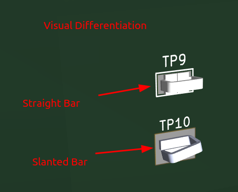
Similarly, Keystone 5005 test hooks come in a number of different color coded variants. The part number 5005 indicates red plastic on the test hook; black, white, yellow, and a number of other colors are offered. This color coding is a handy differentiator between signals: you might have a convention where white test hooks correspond to reset signals, yellow test hooks to clocks, etc.
This approach helps quickly identify the function of each test point, reducing confusion and errors during testing.

Want to support KicadTips?
Consider purchasing EE tools or supplies through our Amazon affiliate links. You get quality items at no extra cost, and we earn a small commission.
Whether you need an oscilloscope, solder, or jumper wires - every purchase helps!
Zero Ohm Resistors or Cut Traces
Incorporating zero ohm resistors or cut traces on digital signal buses allows for easy net disconnection and rework. This flexibility is crucial if you’re unsure of the pinout of a UART, SPI, or I2C bus. (UART buses, in particular, frequently fall victim to TX/RX line mix ups.) Having pads that you can disconnect and easily re-wire are especially valuable during an initial board spin, when not all digital interfaces have been brought up yet.
- Zero Ohm Resistors: Preferred when paying for assembly as they eliminate the need for cutting the PCB, providing ready-made pads for tacking bodge wires onto.
- Cut Traces: Ideal when populating the board yourself, as they reduce the number of components to populate and reflow.
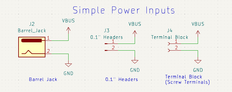
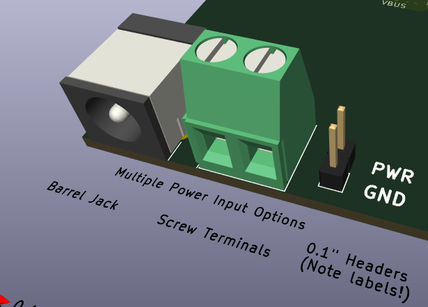
Easy Inputs for Power
Providing easy inputs for power can save time and effort during the testing phase. Common options for power input include:
- Barrel Jacks: Allows a design to be powered from a simple AC-DC wall wart, which are available from suppliers like Digikey in nearly every DC voltage and power rating. These are often are preferred over screw terminals for low-current applications.
- 0.1” Headers: The humble 0.1” header is a convenient power input option that is cheap, easy to install, and easy to clip on to. It’s also quite compact - easily the smallest of the options we’ve shown here. Headers of this kind can withstand a respectable 2[A] of current, too. The main drawback with this method is that it is easy to get power and ground backwards in this configuration. Be sure to include clear silkscreen labels if you choose this method of power delivery!
- Screw Terminal Blocks: Ferrule crimped wires into screw terminals is the power delivery method of choice in many industrial systems. This makes for secure electrical connections that are easy to wire to bulkhead or panel mount connectors - a very common arrangement in industrial PCBs. These can prove simpler than barrel jacks when you are dealing with power inputs from a casing-mounted connector with a prefabricated cable assembly. However, they come with the same drawback as 0.1” headers - the basic models have no poka-yoke features to ensure power and ground are connected to the correct pins. Clear labeling is essential!
Easy Inputs/Outputs for Signals
Using BNC or SMA connectors for signal inputs/outputs allows direct connections to oscilloscopes, function generators, and spectrum analyzers. This facilitates quick and reliable testing of signal integrity and performance. For RF, or very low magnitude signals, it can be the only way to connect your circuit to test equipment. Sometimes, oscilloscope probes just don’t have the bandwidth or noise rejection!
Library of “Known Good” Schematic Snippets
Reducing design risk is a hallmark of good engineering design practice. The least risky board design to work with is always one you have worked with before. Maintaining a library of “known good” schematic snippets, such as JTAG pinouts and UART connections, ensures that you have reliable references for commonly used interfaces. This saves a ton of time and headaches during the design and debugging phases.
In some places, KiCad takes care of some of this “known good” hassle for you. The ARM_JTAG_SWD10 primitive is a great example of this. This component provides the correct SWD pinout used by many, many ARM MCU development boards.
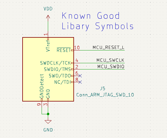
This debug connector maps nicely to a common SamTec FTSH keyed 0.05” header - perfectly poka-yoke’d to ensure that there is only one right way to attach your debugger to the target!
Spare Footprints for Pullups, Pulldowns, Bypass, and Series Components
Add unpopulated footprints for pullup, pulldown, or bypass components. These footprints provide flexibility during testing and debugging, allowing you to add or remove components as needed to optimize circuit performance. This is particularly useful in early board revisions, where you may need to work on peripheral components that don’t yet have software support yet. Instead of waiting for your firmware engineers to toggle a GPIO, you can rework a few components and work on peripheral bringup while your software counterparts mutter over bit macros (or whatever else it is they do).
Add 0.1” headers or jumper pads onto RESET or Enable lines to facilitate bringup and debugging without software support. This feature allows you to manually control these lines, enabling easier troubleshooting and testing.
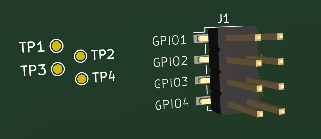
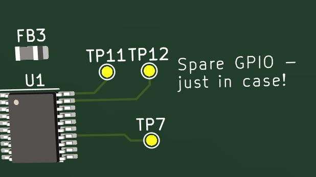
Test Points for Spare MCU GPIO
It is always a good idea to break out extra microcontroller GPIO to test points. Spare GPIO frequently come in handy if requirements change, or an additional IO is needed to prototype a feature. A spare GPIO output or input is a useful thing to have lying around in a pinch!
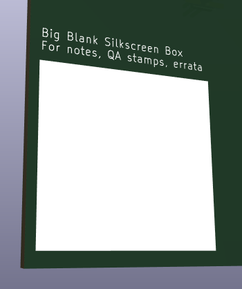
Silkscreen Box for Notes
Include a silkscreen box on the board for taking notes with a Sharpie. This can help track changes and modifications during the testing process, making it easier to document and communicate issues and solutions.
Bodge Wire Holes
Add a hole in the board to run bodge wires from one side to the other without going around the edge. This feature simplifies rework and modifications, allowing for cleaner and more efficient wire routing.
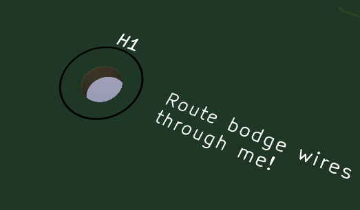
It’s particularly helpful in designs that include a co-designed casing, where it may not be possible to bodge a wire around the board edge due to casing interference. A hole in the board - even a small one - gives you an option where you previously had none!
Dual-Mount Footprints
Use footprints that can accommodate both THT and SMT components. This dual-mount capability provides flexibility in component selection, making it easier to switch between through-hole and surface-mount technologies based on availability and design requirements.
This was an invaluable feature during the semiconductor supply shortfalls of the early 2020s; multiple part footprints were the only things standing in the way of many products shipping!
Software-Readable Board Version Numbers
Nearly every printed circuit board has some kind of programmable component on it these days. Whether a humble microcontroller, or an embedded Linux system, almost every circuit design relies, in some part, on software. It’s frequently critical to maintain some level of compatibility between the software and hardware. Thus, it’s important to have a method for your software to understand what version of hardware it is running on.
The simplest way to code for this on a printed circuit board is often a very simple array of resistor pullups/pulldowns on a dedicated set of microcontroller GPIO pins. This gives you four bits of software-readable version field for your system - a total of 16 hardware versions. While this doesn’t seem like much, this can easily provide enough versioning information for several years of printed circuit board versions - even at the breakneck pace of 6 circuit board revisions per year!
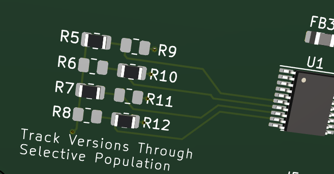
However, this method has some drawbacks:
- It doesn’t provide a very rich set of information - just a simple number indicating board version.
- It’s GPIO intensive - four GPIO can potentially be a lot of space on a very pinout constrained design.
A simple way to get around this is to use an EEPROM to provide software-readable board version information instead of basic GPIO. This is slightly more expensive, but allows for a ton of information to be kept local to the board.
Some ideas of what you can include in a version control EEPROM:
- Board version number,
- Git hashes of your PCB’s KiCad repository
- Coded flags for board features (e.g.
DAC_ENABLED,I2C_BUS_2,BUG-2542 fixed) - Calibration data for onboard DACs or radios
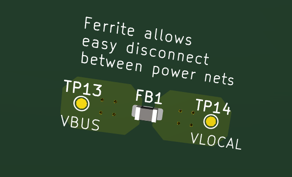
Ferrites at Power Entry/Exit Points
Use ferrites at the entry and exit points of power domains to isolate power sections for debugging. Ferrites help reduce noise and interference between power domains, improving the overall stability and performance of the circuit during testing.
By incorporating these features into your circuit board designs, you can significantly enhance the efficiency and effectiveness of your testing and debugging processes.
Conclusion
Did we miss your favorite PCB debug bringup trick? Don’t hesitate to tell us about it - shoot us an email at kicad.tips@gmail.com and let us know! We’ll follow up here in a few weeks with updates based on your feedback!