How to Generate Gerbers in Kicad
Here’s a concise guide to generating Gerber files in KiCad. We’ll start from your open project’s your finished PCB file, in PCBnew.
This guide assumes all layers and elements are correctly placed and connected. It is wise to run DRC (Design Rule Check) to catch any design errors before this step (from the Inspect menu).

Want to support KicadTips?
Consider purchasing EE tools or supplies through our Amazon affiliate links. You get quality items at no extra cost, and we earn a small commission.
Whether you need an oscilloscope, solder, or jumper wires - every purchase helps!
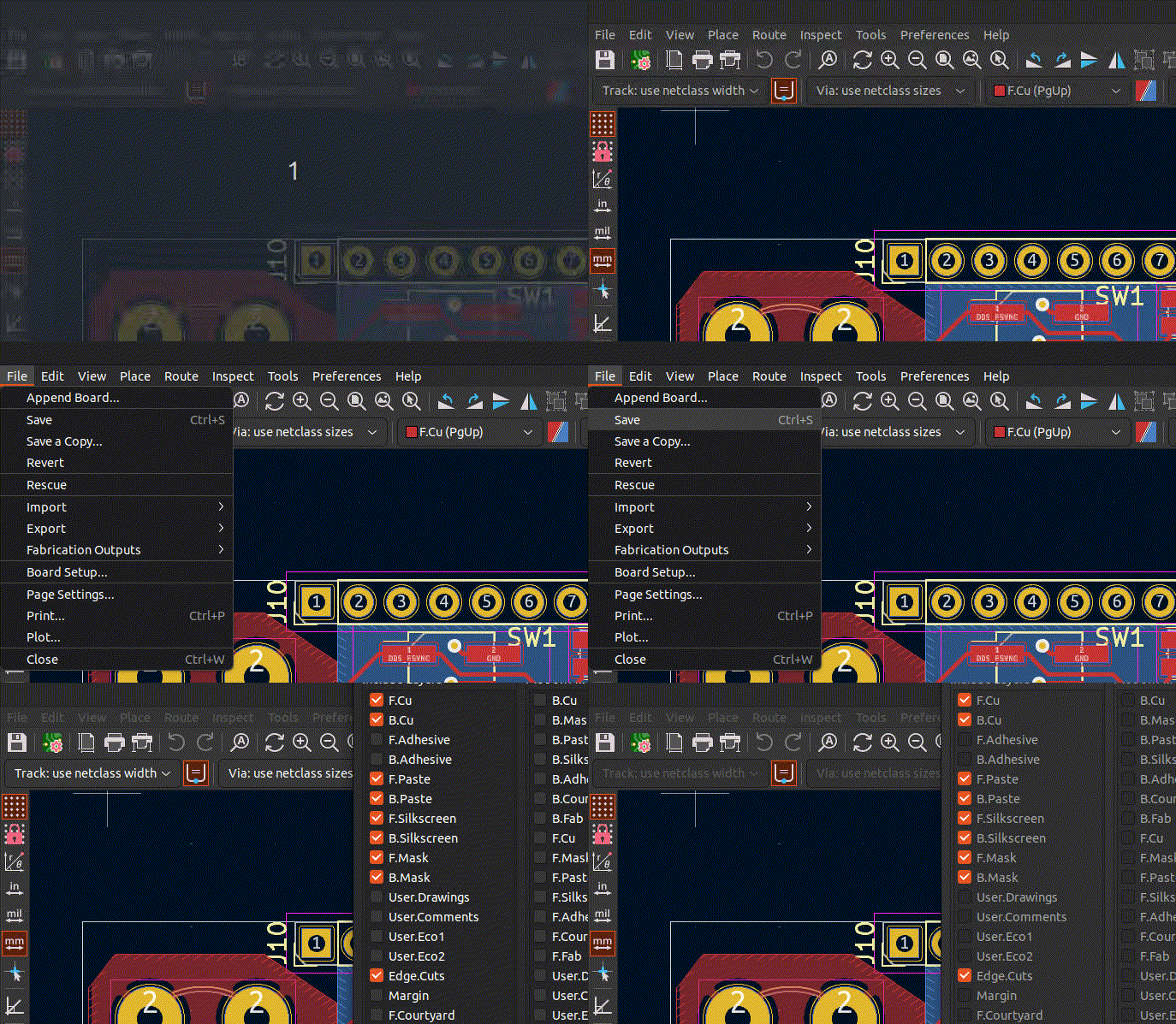
Step One: Open The Plot Window
- Go to
File>Plot.
Step Two: Configure Your Layer Plots
- In the Plot window:
- Set the
Output Directoryto where you want the Gerber files saved. -
Choose the layers you want to export (e.g., F.Cu, B.Cu, F.SilkS, B.SilkS, F.Mask, B.Mask, Edge.Cuts).

- Ensure
Gerber Optionsare set:- Enable “Use Protel filename extensions”.
- Enable “Exclude PCB edge layer from other layers”.
- Set the
Step Three: Plot Your Layers
- Click the
Plotbutton to generate the Gerber files.
Step Four: Generate Drill Files
- In the Plot window, click
Generate Drill Files.
- In the Drill Files Generation window:
- Ensure the
Output Directoryis correct. It is common practice to include this in the same directory as your gerber files. - Select
PTH and NPTH in single file. - Set other options as needed.
- Ensure the
- Click
Generate Drill File.
Step Five: Verify Your Gerbers
- Use a Gerber viewer (such as GerbView, included with KiCad) to open and check the generated files for accuracy.
- It is sometimes recommended to use a separate gerber viewer, in order to catch errors that may occur as a result of two programs using the same rendering engine.
Your Gerber files are now ready for manufacturing!